How to remove the copper layer/film from a PCB
1 remove the copper film 2 stick it to the foil, that you can laminate 3 put the "ribbon cable pattern" on the film and ETCH it 4 laminate it and cut the just the top of the laminate foil at the ends, so you have clear cooper for the contacts, but the bottom laminate film as a supportAll PC boards have a thin layer of copper that adheres to them This copper is the wiring or traces for conveying an electrical current to all of the components that are soldered onto the board You can recycle used PC boards, once you have removed all of the electronic components What's left are the copper traces, which you can strip and send to any recycling center or scrap yard that deals How to Remove Copper From a PC Board Our Pastimes A milled printed circuit board Printed circuit board milling (also: isolation milling) is the process of removing areas of copper from a sheet of printed circuit board material to recreate the pads, signal traces and structures according to patterns Printed circuit board milling WikipediaI'm seeking advice on how to remove the unwanted copper from the edge of the cut PCB internal planes My first thought was to use a highspeed downcut router bit but, upon reflection, that will probably push the edges of the copper planes together and cause short circuits Another thought is to use a flatbottomed vessel with a very shallow depth of PCB etchant, then stand the circuit board How to remove copper from inner planes on cut PCB 2 Use conductive ink on a nonconductive board to remove the unwanted copper This silkscreening process uses ink that conducts electricity to protect the copper traces An electrochemical reaction then removes the unprotected copper 3 Photoengrave the PCBHow to Remove Metals From Printed Circuit Boards

Stripping and Etching Process of PCB Sierra Assembly
While making PCBs, a layer of copper is added on the substrate Sometimes, both the sides of the substrate are covered with copper layers PCB etching process is carried out to get rid of the excessive copper, and only the required copper traces are left behind after the etching process The etching process can be carried out in a number of waysThe loose catalytic layer formed on copper foil can be eliminated by using colloidal palladium activation solution Moreover, the colloidal palladium activation solution has very good activity and obviously improves the quality of electroless copper plating layer Therefore, it has been widely used in the hole metallization process of PCBDetailed Procedures of Plating Copper for PCB Processing Etching is probably the easiest and most cost effective Etching is the process of chemically removing the unwanted copper from a plated board You must put a mask or resist on the portions of the copper that you want to remain after the etch These portions that remain on the board are the traces that carry electrical current between devicesPCBs Fabrication Methods All PC boards have a thin layer of copper that adheres to them This copper is the wiring or traces for conveying an electrical current to all of the components that are soldered onto the board You can recycle used PC boards, once you have removed all of the electronic components What's left are the copper traces, which you can strip and send to any recycling center or scrap yard that deals How to Remove Copper From a PC Board Our PastimesIn PCB fabrication, etching is a process of removal of unwanted copper (Cu) from the circuit board The unwanted copper is nothing but the noncircuit copper that is removed from the board As a result, the desired circuit pattern is achieved During this process, the base copper or the start copper is removed from the board Before the etching process, the designer’s desired image of the Learn About PCB Manufacturing Processes Sierra Circuits

Stripping and Etching Process of PCB Sierra Assembly
Step 10: This completes the etching process of a printed circuit board You can now drill the holes using proper tools with the required drill bit size PCB Stripping Process Post etching process, the copper present on the PCB gets covered either by electroplated tin or tin/lead You can use concentrated Nitric acid to remove the tin Nitric acid is very effective in removing tin, and does In this paper, a novel process to produce copper from ground and concentrated printed circuit board (PCB) powder is presented In this process, a powder sample containing approximately 48% copper and 40% other metals, as well as 12% nonmetallic materials, was anodically dissolved in an acidic copper sulfate solution, while copper ions were simultaneously reduced on the cathode, Direct recovery of copper from printed circuit boards The microetching is the process of roughening the surface in order to create a strong adhesion between the chemically deposited copper and copper substrate The main purpose of this step is to create a coarse active copper surface by removing the oxide on the surface The new active coarse copper will now be able to absorb colloidal palladium wellAnalysis on Plating Copper Process for PCB Recycling Copper From the Spent Tin/Lead Stripping Solution From the Solder Stripping Process: Following the etching process, remove the protective solder plate to expose the copper connections Strip the tin and lead from the solder plate by immersing the printed circuit board in nitric acid or a hydrogen fluoride stripping solution Use electrowinning to recover the copper and lead, as How to Recycle Printed Circuit Boards MCL——Technical Analysis of Plating Copper for PCB Processing Electroless plating is widely used in the printed circuit board (PCB) production and processing which has holes on that and it can also be called PTH(Plate Through Hole), the main purpose is to deposit a layer of copper through a series of chemical treatment methods in the conductive substrate, and then increasing the thickness of Detailed Procedures of Plating Copper for PCB Processing

Recovery of Gold, Silver, Palladium, and Copper from Waste
wt% copper, 004 wt% gold, 015 wt% silver, and 001 wt% palladium The extraction of these metals from PCBs is both profitable and environmentally worthwhile Hence, this study aims to design a commercial process to extract these four metals from PCBs of computers and mobile phones This paper discusses the relevant market analysis and research that led to the selection of these metals and The complex system of copper routes determines the unique role of each piece of printed circuit board Before PCB design, circuit designers are recommended to get a tour of a PC board shop and communicate with fabricators face to face over their PCB manufacturing demands It helps prevent designers making any unnecessary errors from getting transmitted during the design stage However, PCB Manufacturing Process – A Step by Step Guide PCBCartNonfunctional pad features great improvement to PTH copper in the process of manufacturing PCB via wall and plays an effective role in stopping via copper from falling and dealing with quality problems such as via wall crack Of course, NFP features some variables and Removal of Nonfunctional Pads from Inner LayersIn PCB fabrication, etching is a process of removal of unwanted copper (Cu) from the circuit board The unwanted copper is nothing but the noncircuit copper that is removed from the board As a result, the desired circuit pattern is achieved During this process, the base copper or the start copper is removed from the board Before the etching process, the designer’s desired image of the Learn About PCB Manufacturing Processes Sierra Circuits PCB etching is a process of removal of unwanted copper (Cu) from the circuit board When I say unwanted, it is nothing but the noncircuit copper that is removed from the board As a result, the desired circuit pattern is achieved In other words, etching is like chiseling the circuit board If you can think like an artist, the board is a rock, and etching chisels the rock into a beautiful Wet PCB Etching Using Acidic and Alkaline Methods Sierra

How to Recycle Printed Circuit Boards MCL
Recycling Copper From the Spent Tin/Lead Stripping Solution From the Solder Stripping Process: Following the etching process, remove the protective solder plate to expose the copper connections Strip the tin and lead from the solder plate by immersing the printed circuit board in nitric acid or a hydrogen fluoride stripping solution Use electrowinning to recover the copper and lead, as The microetching is the process of roughening the surface in order to create a strong adhesion between the chemically deposited copper and copper substrate The main purpose of this step is to create a coarse active copper surface by removing the oxide on the surface The new active coarse copper will now be able to absorb colloidal palladium wellAnalysis on Plating Copper Process for PCBwt% copper, 004 wt% gold, 015 wt% silver, and 001 wt% palladium The extraction of these metals from PCBs is both profitable and environmentally worthwhile Hence, this study aims to design a commercial process to extract these four metals from PCBs of computers and mobile phones This paper discusses the relevant market analysis and research that led to the selection of these metals and Recovery of Gold, Silver, Palladium, and Copper from Waste Electroless plating is widely used in the printed circuit board (PCB) production and processing which has holes on that and it can also be called PTH(Plate Through Hole), the main purpose is to deposit a layer of copper through a series of chemical treatment methods in the conductive substrate, and then increasing the thickness of the copper layer through subsequent electroplating methods to Detailed Procedures of Plating Copper for PCB Processing There are 2 ways of removing the copper from a board to make traces: The Milling process and the Etching process The Milling process needs really special toolsVery precise Mill equipment is needed (that is dead expensive) so I will just describe this method: A drill enters the copper board, but only half way, just to remove the copper layer from the topHow to Make PCBs Easily : 9 Steps Instructables

What PCB Copper Plating Process is the Best Choice for
Making the Best PCB Copper Plating Process for Your Board Typically, electroless or electroplating is employed to create vias or PTHs Electroless plating does not require electricity; however, a catalyst is required for deposition Electroplating, on the other hand, uses electrolysis where a DC current dissolves a copper rod and the copper is then distributed on the surface When We fed JC 9830 into the aeration basin and chemically bonded the dissolved copper to form a copper sulfide In the inlet of the Secondary Clarifier, we fed JC 1687 The results of our study indicated that we could remove 94% of the dissolved copper and 70% of the dissolved zinc from the effluent Please note that all the data collect was the Removing Dissolved Copper from wastewater effluent Hi, I always have a very annoying problem when doing multilayer boards in Altium that I don't know how to get rid of apart from manually patching it with fills It happens when I have a multilayer board with internal planes (negative planes moslty used for power and ground), and some unconnected via pattern makes altium generate the mess you see in the attached picHow do I remove necks and dead copper on internal planes
- energy saving road cleaning machine
- gold crusher equipment supplier
- various type of husk chips cutting machine
- mill for grinding rotary shears
- reaction of al mining
- kinematics general kinematics mining equipment
- cement and crusher plant in pakistan
- STONE MACHINE HAMMER CRUSHER
- reducing the size of arse limestone using crushing plant
- chinese canola crushers
- gravel quarry equipment manufacturer
- separation of haematite from gypsum
- st of bauxite ore jaw crusher for sale
- is what is the mposition of cement
- impact crusher price model pf
- ball tube mill photos
- jaw rock crusher sale in South Africa on hot sale
- SANDIK 880 CH CONE CRUSHER IN MINING
- toggle jaw crusher advantages
- skillmill portable sawmill for sale
- Coal Mine Contractors Number In Pakistan
- 2015 top sell china super thin mill pdf
- calcite beneficio calcite production used for producing cement
- transporting minnig equipment to pperbuilt
- NATURAL ZEOLITES TREATMENT
- mobile ne crusher plant price from india
- mobile crusher output
- pdf asphit crusher neyor belt plant
- PRINCE GEORGE MINING EQUIPMENT AND SUPPLIES
- Made Wndian Stone Granding Ball Mill
- Cedar s Mvp 450 Manganese Mtm Crusher
- vertical roller mill for bentonite grinding
- bullock gold mining case study 725000000
- project st of 100tph stone crusher
- premier wonder le top wet grinder 110v in indian
- crusher plate manufacturers
- Grinding Mill Trucks Amp Buses Motoring South Africa
- basalt aggregate crushing plant
- ACTION MINING IMPACT MILL VIDEO
- harga air micro grinder china
Stationary Crusher
Sand making equipment
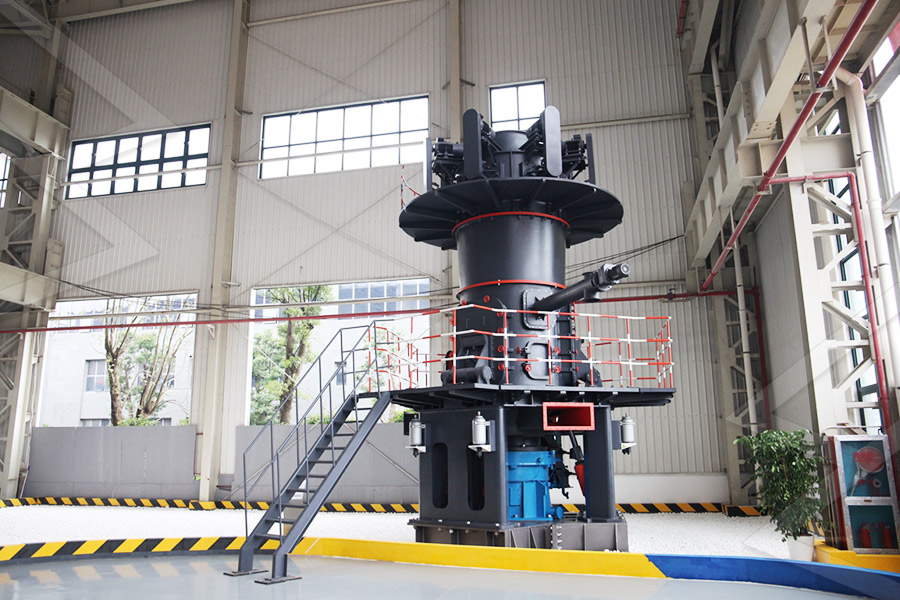
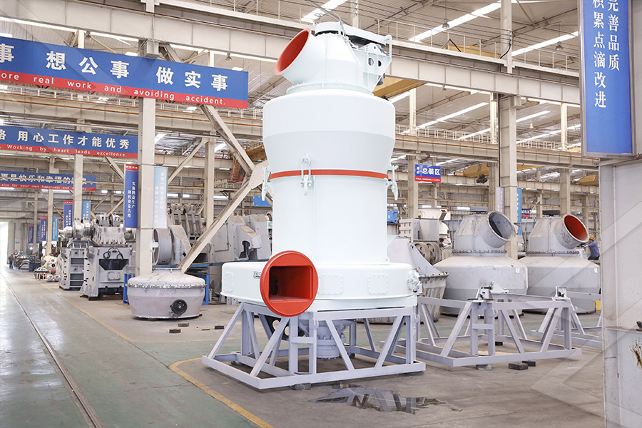
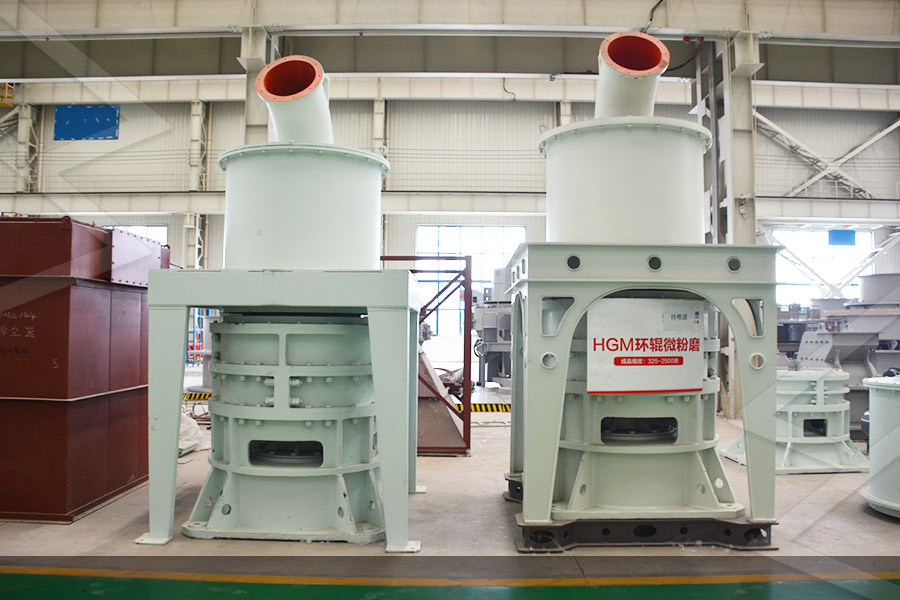
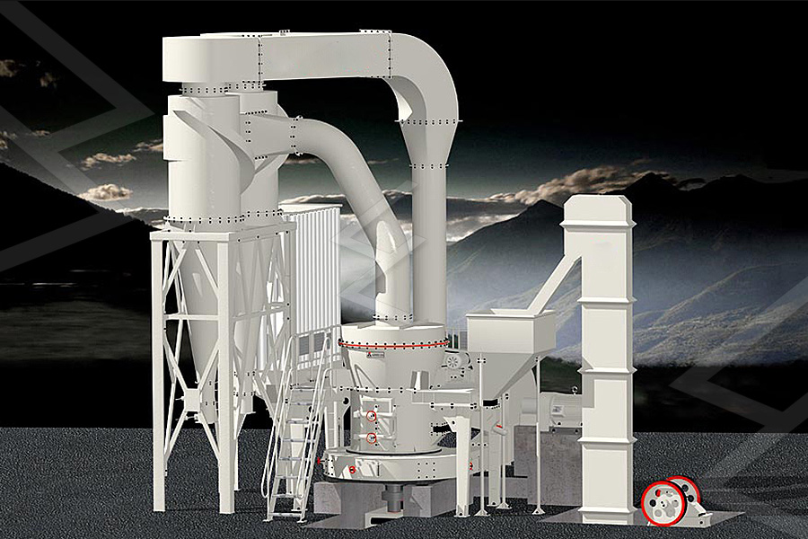
Grinding Mill
Mobile Crusher